Photoelectric effect stands as one of most fundamental phenomena on physics. It shows quantum nature of light and forms basis for countless tech apps. When electromagnetic radiation interacts with matter, it brings changes to material’s electrical traits via electron liberation or excitation. This phenomenon has several distinct mechanisms. They together shape our grasp of light - matter interactions and enable many photodetection devices to work.

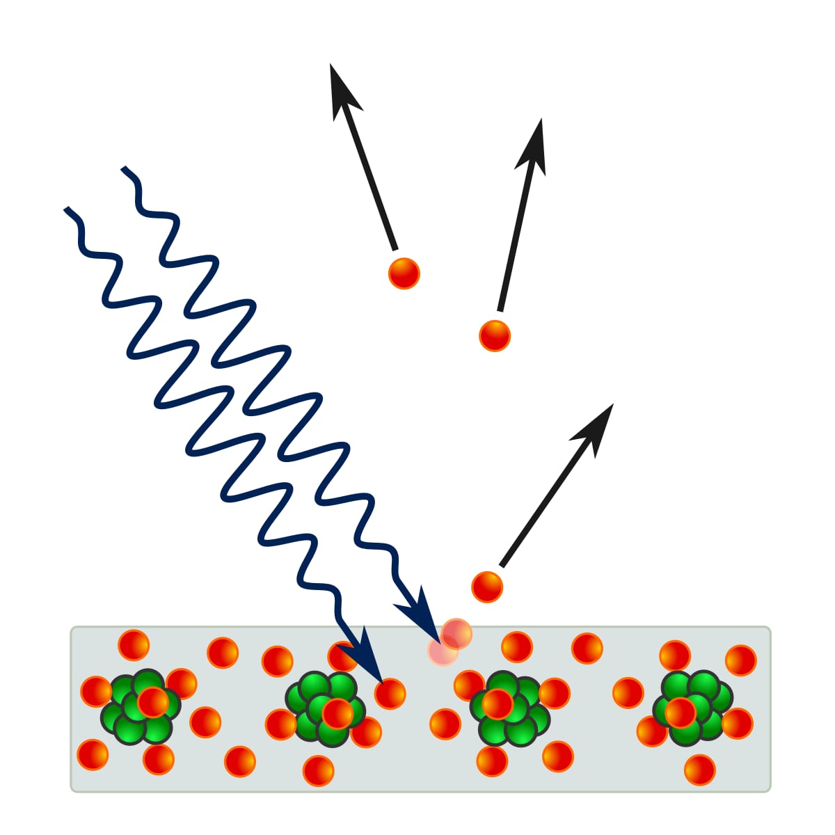
Diagram shows external photoelectric effect where light photons make electrons emit from a metal surface.
Photoelectric effect has two main forms. Each form features distinct electron behaviors and material needs. External photoelectric emission happens when photons give enough energy to fully remove electrons from a material’s surface, pushing them into surrounding medium. In contrast, internal photoelectric effects involve electron excitation inside the material itself, without fully removing them from atomic lattice.
This key difference decides not only involved physical mechanisms but also practical apps and tech implementations of each type. External effects usually need vacuum environments and are sensitive to surface conditions. Internal effects work in solid - state materials and rely on bulk semiconductor properties.
External photoelectric effect takes place when incident photons have energy exceeding material’s work function — the minimum energy barrier electrons must cross to escape from surface. This quantum mechanical process follows Einstein’s photoelectric equation: E = hν - W₀. Here, E is kinetic energy of emitted photoelectrons, hν is photon energy, and W₀ is work function.
The process has several features that set it apart from classical electromagnetic predictions. First, electron emission starts right when illuminated, no matter light intensity. Second, max kinetic energy of photoelectrons depends only on photon frequency, not intensity. Third, below a material - specific threshold frequency, no electrons are emitted no matter light intensity.
Different materials have different work function values, directly affecting their photoelectric properties. Alkali metals like cesium (2.1 eV) and sodium (2.28 eV) have relatively low work functions, making them fit for visible light detection. On the contrary, noble metals such as platinum (6.35 eV) and gold (5.1 eV) need ultraviolet radiation for photoelectron emission.
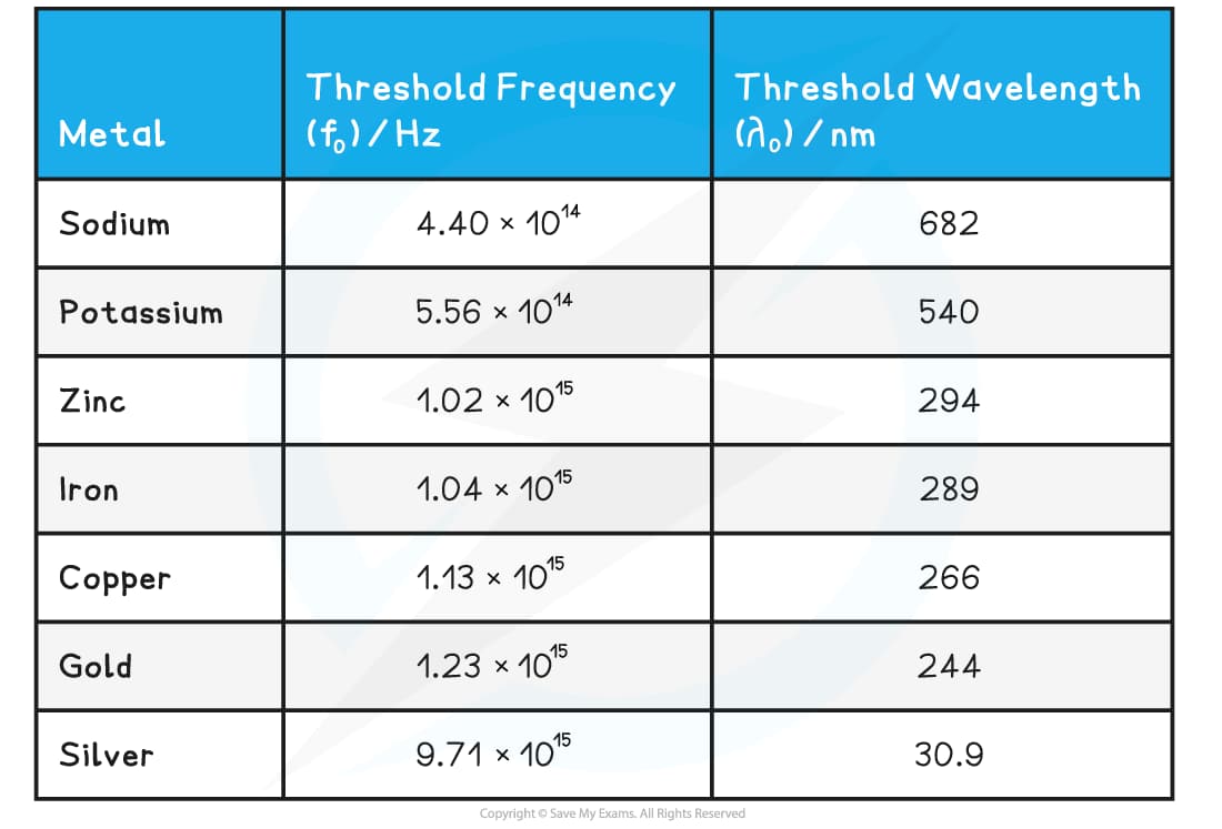
Table shows threshold frequency and wavelength for various metals related to photoelectric effect.

Threshold frequency ν₀ = W₀/h decides the longest wavelength that can trigger photoelectric emission. Materials with lower work functions react to longer wavelengths. Those with higher work functions need shorter, more energetic photons. This relation directly affects spectral sensitivity and app range of photoelectric devices.
External photoelectric effects form operational basis for many vacuum - based photodetection systems. Photomultiplier tubes use photocathodes with low work functions to turn incident photons into electron cascades, getting great sensitivity for low - light detection. Vacuum photodiodes use similar ideas but work without internal amplification, giving linear response traits good for precise measurements.
Image intensifiers and night vision devices use external photoelectric emission to turn invisible infrared or low - level visible light into detectable signals. These apps especially gain from instant response and low noise traits of vacuum photoelectric devices.
Internal photoelectric effects happen in semiconductor materials when absorbed photons give enough energy to move electrons from valence band to conduction band. Unlike external emission, these electrons stay in the material but become mobile charge carriers that can conduct electricity. The minimum photon energy needed equals material’s bandgap energy Eg, usually ranging from 0.3 eV to 3.5 eV for common semiconductor photodetectors.

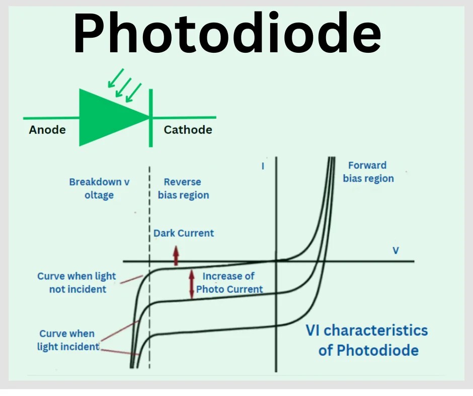
VI characteristics of a photodiode show current response under light and dark conditions in forward and reverse bias areas.
When photons with energy hν ≥ Eg are absorbed, they create electron - hole pairs — negatively charged electrons in conduction band and positively charged holes in valence band. Both charge types help with electrical conductivity, allowing detection via changes in current or voltage.
Choice of semiconductor material decides spectral response range of photodetectors. Silicon (Eg = 1.12 eV) responds to wavelengths up to about 1.1 μm, covering visible spectrum and near - infrared area. Germanium (Eg = 0.67 eV) extends sensitivity to 1.8 μm, good for telecom apps.
Relationship between bandgap energy and detection wavelength for semiconductor photodetector materials.
For longer wavelength detection, compound semiconductors offer lower bandgap energies. Indium gallium arsenide (InGaAs) gives sensitivity up to 1.7 μm with great quantum efficiency. Lead salt materials like lead sulfide (PbS) and lead selenide (PbSe) allow mid - infrared detection beyond 3 μm, though often needing cooling to cut thermal noise.
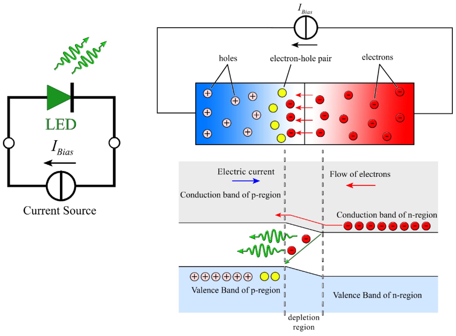
Internal photoelectric effects are put into use via various semiconductor device structures. p - n junction photodiodes use built - in electric field at junction interface to separate photogenerated electron - hole pairs, creating measurable photocurrents. p - i - n photodiodes add an intrinsic semiconductor layer to increase depletion region volume, boosting quantum efficiency and response speed.

Diagram of a p - n junction LED circuit and internal photoelectric effect shows electron - hole recombination and light emission at depletion region.
Avalanche photodiodes use high reverse bias voltages to create impact ionization, multiplying photogenerated carriers and getting internal gain. This amplification allows detection of extremely low light levels while keeping fast response times fit for high - speed optical communications.
Internal photoelectric effects show in two main modes: photoconductivity and photovoltaic generation. Photoconductivity means increased electrical conductivity due to extra charge carriers made by photon absorption. This effect is basis for photoconductive detectors and photoresistors used in light sensing apps.
The photovoltaic effect generates electrical voltage across p - n junctions when lit, forming foundation for solar cells and self - powered photodetectors. This phenomenon lets light energy turn directly into electrical power without external bias, making it key for renewable energy apps.
External photoelectric effects have little temperature dependence as electron emission mainly depends on photon energy rather than thermal excitation. Vacuum photodetectors usually work well at room temperature with stable traits across wide temperature ranges.
Internal photoelectric effects are more sensitive to temperature because of thermal generation of charge carriers. At high temperatures, thermal energy can push electrons across bandgap even without photon absorption, creating dark current that lowers detection sensitivity. Materials with very small bandgap energies, like those used for mid - infrared detection, need cooling to liquid nitrogen temperatures (77 K) or thermoelectric cooling to suppress thermal noise.
Modern cooling tech, including Stirling coolers and thermoelectric coolers, let sensitive infrared detectors be used practically while keeping acceptable power use and system complexity.
Photoelectric effects enable a wide range of tech apps across scientific instrumentation, telecommunications, imaging, and energy conversion. CCD and CMOS image sensors use internal photoelectric effects in silicon to capture digital images with great spatial resolution and sensitivity. Fiber optic communications depend on high - speed photodiodes to turn optical signals back to electrical form.
Emerging apps include quantum dot photodetectors that use quantum confinement effects to achieve normal incidence detection in infrared wavelengths. Two - dimensional materials like graphene and transition metal dichalcogenides offer new chances for ultrafast, broadband photodetection with CMOS compatibility.
Photoelectric effect includes fundamental quantum mechanical processes that bridge gap between electromagnetic radiation and electronic devices. External photoelectric emission gives foundation for sensitive vacuum - based photodetectors. Internal photoelectric effects enable solid - state revolution in imaging, communications, and energy conversion. Understanding these mechanisms and their material dependencies keeps driving innovation in photodetection tech, enabling new apps in emerging fields like autonomous systems, quantum tech, and advanced sensing platforms.
Continued development of new materials and device architectures promises more advances in sensitivity, speed, and spectral coverage, making sure photoelectric effects stay central to future tech progress. From quantum nature of light found through photoelectric studies to practical devices that shape modern life, this phenomenon shows successful translation of fundamental physics into transformative tech.
Contact: Jason
Phone: +8613337332946
E-mail: [email protected]
Add: Hangzhou City, Zhejiang Province, China