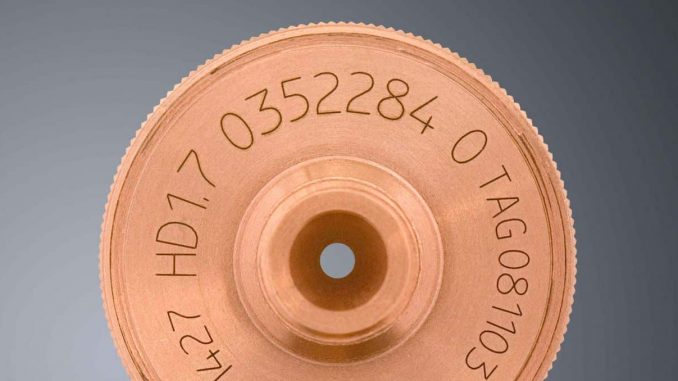
In my three decades of metal fabrication, I’ve seen laser marking reshape how manufacturers add permanent, high-precision identifiers to parts. Copper’s excellent electrical and thermal conductivity makes it indispensable across industries—but its high reflectivity causes most laser light to bounce off, leaving faint or no marks. At NANO MARK, we’ve mastered the art of concentrating intense, ultrashort laser pulses onto copper to create clear, durable engravings without slowing production or harming the environment. Below, I share my hands-on approach, real-world applications, and SEO-friendly tips—concise, engaging, and enriched with useful links.

Copper reflects over 95% of near-IR laser light, so a standard beam leaves barely a trace. Early on at NANO MARK, I discovered that three parameters are essential:
Peak Pulse Power: Breaks through surface oxides.
Pulse Width Control: Tunes depth from a light tint to deep engraving.
Small Spot Size (30–50 µm): Concentrates energy on a pinpoint.
By delivering powerful, focused bursts, we force the copper to absorb enough energy to form permanent contrast. This expertise underpins every NANO MARK system, from our compact desktop units to inline production workstations.
1. Permanent, High-Contrast Identification
I etch serial numbers, QR codes, and logos that endure cleaning, polishing, and heat. Our marks stay crisp for decades, ensuring traceability and anti-tamper protection.
2. Versatile Surface Processing
Beyond marking, we texture or roughen copper surfaces to improve adhesion or clean joints before soldering. Precise laser pulses remove oxides only where needed, keeping surrounding areas intact.
3. Streamlined Workflow
Laser marking integrates seamlessly into production lines. Parts emerge ready for polishing or assembly, cutting handling steps and boosting throughput.
4. Eco-Friendly Operation
No inks or chemicals. NANO MARK laser systems conserve energy, generate no toxic waste, and minimize wear on optics and mechanics.
| Application | Benefit |
|---|---|
| Electronics wiring | Traceable, tamper-proof serial codes |
| Automotive heat exchangers | Durable IDs that survive harsh conditions |
| Jewelry and coin minting | Fine decorative engraving |
| Medical instruments | UDI-compliant permanent marking |
Surface Cleaning
Wipe copper with isopropyl alcohol to remove oils and debris.
Laser Selection
Choose a 1 070 nm fiber laser for superior absorption vs. CO₂ systems.
Parameter Tuning
Set peak power above the ablation threshold, adjust pulse width, and select a 50 µm spot-size lens for fine detail.
Test Marking
Engrave small patches, inspect under magnification, and refine settings.
Production Run
Once tests pass, batch-mark parts at full speed.
At NANO MARK, we provide turnkey laser marking systems tailored to your copper applications. From compact desktop units to in-line production workstations, our machines deliver award-winning precision, reliability, and ease of use.
Feel free to explore our website or reach out with questions—let us help you create lasting value with precision copper laser marking.
Visit our News page for the latest product announcements and customer success stories: codingmachine.net/news.html
Explore our full lineup of marking and coding machines—including Fiber Laser, UV Laser, and Inkjet models—on our Product page: codingmachine.net/coding-machine.html
Contact: Jason
Phone: +8613337332946
E-mail: [email protected]
Add: Hangzhou City, Zhejiang Province, China